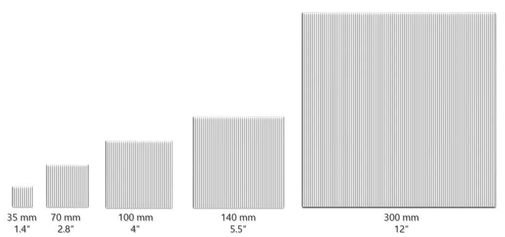
This is the biggest micro optics wafer worldwide, which is 12 inches (300mmx300mm).
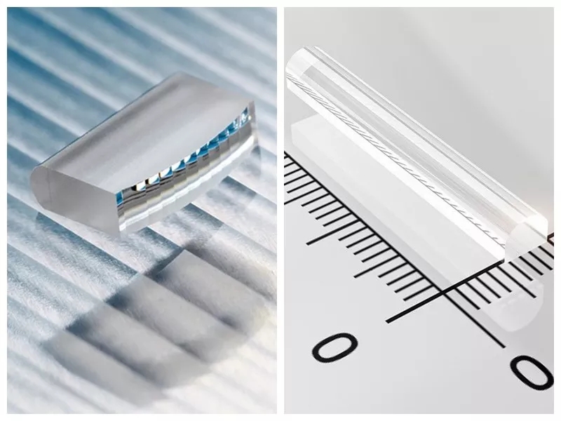
Our micro optics is made by wafer level simultaneous structuring process with complementary?polishing, and could achieve 49 different shapes at the same time. In each of these shapes, there are micro-scale or nano-scale structures. By reflection and refraction, photons are delivered to the right place, at the right time, achieving high efficiency of beam transmission.
Our micro optics could be used for the fast axis and slow axis collimation of diode lasers, achieving very small divergences angle in both fast axis and slow axis, which are applied in solid state lasers and fiber lasers for beam controlling and shaping. Our micro optics could also be used for beam shape transformation. For example, a line beam could be transformed into a square or a circular beam, or a symmetric beam such as circular beam could be asymmetric beam.
In other words, by beam shaping of our micro optics, we could transform a symmetric beam into a line or any designed beam shapes, or an asymmetric beam into circular or square beam.
For the application of automotive LiDAR, consumer electronics, information technology, 3D sensing, machine vision, etc, our micro optics are used for beam controlling, in order to get the designed beam shapes of customers, and get certain angle or field of view (FOV), just like human eyes.
The advantages of our micro optics are superior uniformity and very high efficiency, normally above 90%. The key feature of our technology is that instead of being diffractive optical element (DOE), our micro optics is called refractive optical element (ROE), without ZERO order, namely no hot spot. For the applications such as LiDAR and consumer electronics, this feature will be beneficial to eye safety, which is a very unique feature of our technology.


 Return