Laser World of Photonics China 2025 will be held from Mar 11-13, 2025, at the Shanghai New International Expo Center, Shanghai, China. We sincerely invite you to visit our booth #N5.5368, to explore our high-power diode laser components and materials, laser optics components, as well as photonic application solutions for optical communications, consumer electronics, automotive, pan-semiconductor, and medical & health.
New Product
Focuslight is unveiling multiple new products for the first time at LASER World of PHOTONICS CHINA. We warmly welcome you to visit and exchange insights with us!
980/1470nm Conduction-Cooled Diode Laser with High Power Output, Low Thermal Resistance and Ultra-Low Smile
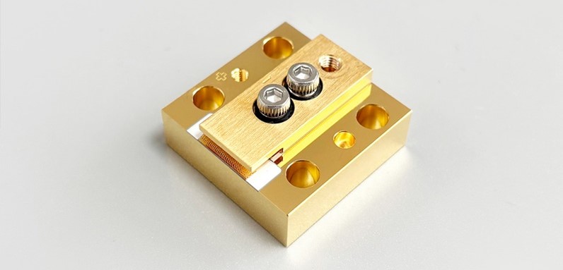
The newly launched LCS series with 100W output at 980nm and 30W output at 1470nm feature conduction cooling designs based on Focuslight’s proprietary bonding technology. Our innovative bonding approach addresses various challenges such as thermoelectric migration, fatigue resistance and thermal resistance, achieving an ideal balance of low stress, low thermal resistance, and ultra-low Smile effects, offering cutting-edge solutions for various application fields including?scientific research, laser equipment manufacturing, biomedical applications, precision ranging, and LiDAR systems.
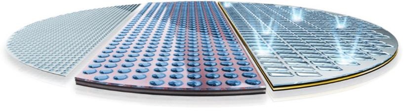
Silicon and Fused Silica Lenses and Lens Arrays Designed for Optical Transceivers and Separated TOSA / ROSA Scenarios
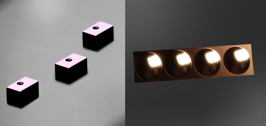
This product featuring their?high precision?and consistency, these lenses and arrays are optimal for focusing, fiber array collimation, and coupling functions in the next-generation optical communication applications like transceivers and separated TOSA / ROSA scenarios. They offer stable coupling and collimation performance at a?competitive price, even under the stringent requirements of high-speed optical modules. We also provide simulation services to our customers to optimize product designs based on simulation results, targeting even higher optical performance.
V-Groove Arrays for Multi-Channel Optical Communications with Flexible Designs
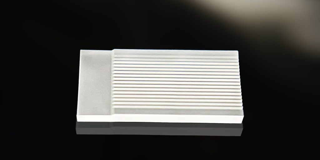
Leveraging Focuslight’s unique wafer-level synchronized structuring process, our V-grooves are made naturally fit for various optical communication applications such as fiber optic connectors, PLC splitters in FTTX networks, AWGs in WDM systems, and optical modules. The product features high precision and consistency with cumulative pitch tolerance within ±0.5μm for 32 channels and within ±1μm for 96 channels. Additionally, it offers a variety of material, pitch, and angle options, allowing different pitches and angles to be implemented within the same product. This makes it particularly well-suited for flexible multiple channel designs and large-scale production, meeting the stringent requirements of the optical communication industry for optical components.
Wafer Level Optics (WLO), Wafer Level Stacking (WLS), and Wafer Level Integration (WLI) for Consumer Electronics and Further Emerging Applications
Wafer Level Optics (WLO) technology, characterized by the precision and efficiency of semiconductor processes, enables the high-volume and highly accurate replication of lenses on entire glass wafers. Within this, lens wafers can be flexibly diced into individual WLO components tailored for specific applications.
Wafer Level Stacking (WLS) technology allows for the micron-level precision stacking of multiple lens wafers, which are then diced into individual micro-optical imaging lenses. During this process, additional functionalities such as apertures, coatings, and spectral filters can be integrated, ensuring miniaturization and high-precision optical components while significantly improving production efficiency and scalability.
Wafer Level Integration (WLI) enables the seamless integration of chip-scale packaged (CSP) sensors into ultra-thin, optically sealed, working modules. This innovative approach not only enhances design flexibility and space utilization but also results in a more compact and efficient optical module. More importantly, it provides an ideal reflowable solution for CSP sensors, ensuring exceptional stability and reliability throughout the manufacturing process.
These advanced technologies are widely applied in the production of advanced optical components, including plano/hybrid optics, projection/imaging optics, diffractive optical elements (DOE), and microlens arrays (MLA). These components play a crucial role in applications such as augmented reality (AR) and virtual reality (VR), automotive projection lighting systems, disposable endoscopes for medical use, and industrial robotics.
We look forward to seeing you at LASER World of PHOTONICS CHINA 2025, Booth #N5.5368!


 Return